Wafer Probe
The specific implementation of wafer probing depends on:
- the component testing needs
- variability of the fab process in terms of yield
- the required quality and reliability level
- the economic model in terms of time and cost relative to all of the above factors.
Why is 100% wafer probing needed?
Use in bare form
Where the component use is in the bare die form as either hybrid or multiple-chip-module (MCM), multiple-chip-package (MCP) it’s strongly recommended that a wafer is 100% probe tested because this is the only test that will be applied before the device is operating in the application. Additionally where the application comprises multiple bare die, the risk of using an untested die amongst tested die is a yield risk multiplier at the module level and potential weak link.
For military, automotive, space and most medical applications 100% probing of bare die is an automatic requirement and integrated into industry standards.
For commercial integration of bare die into modules, there is no absolute fixed standard and variations can be found of process flows which loosely are termed “Known Good Die” (KGD). The definition and understanding of this term KGD is frequently misunderstood. If you think you want “Known Good Die” please contact us to discuss the requirement because it is an application and product specific answer.
Wafer level probing is also used to identify and select out different electrical grade die from within a given wafer, this is known as electrical “binning”. This can be useful where certain parameters need to be assured or a higher grade needs to be selected akin to the equivalent packaged part version of the product.
Use in discrete package assembly
Where the cumulative cost of assembling and testing rejects from a wafer is more than the cost of implementing 100% wafer probe. This tends to occur where a part is new, is relatively uncharacterised or has a natural yield variation due to the fab process. It also may also be justified where the economic cost of the semiconductor wafer is high to provide additional process reliability.

When is 100% wafer probing not needed?
The predominant reason to avoid 100% wafer probing is commercial cost. The prime objective of probing is early removal of reject die from the production flow early before assembly and package test to avoid a higher aggregated loss. However, mature fab processes, simpler devices or components with consistently high yield history may not require 100% wafer probe testing and instead, sample probe testing may provide sufficient confidence that a given wafer will exhibit minimal rejects after assembly and test. In these cases the cost saved by not doing 100% wafer probe is more than the total cumulative cost of throwing away tested assembled components later. Rather than no probe at all some wafer manufacturers may, as a compromise, choose to perform a sample probe across the wafer and apply statistical analysis correlated with assembly yields.
Occasionally customers will need to use the bare die form but may be restricted because the OEM will only output either sample tested wafers or 100% un-probed wafers, in these situations Reltronix can offer a 100% wafer probe test flow to enable the product use in the bare die form.
When is wafer probing not a design consideration?
- Some modern semiconductor chip designs may not even consider probing as part of their design flow at all and this can present challenges.
- Pad structure or pad metal may be ill fitting or incompatible with probe contacts due to only expectation of mass production test in the fully assembled package version only
- Chip design may feature active circuit structure under bond pads due to only expectation of mass production test in the fully assembled package version only
- The die may be bumped and may also contain active circuit structure under the bumps
- Due to use of monolithic e-trim block circuitry some IC are only intended to be fully tested and calibrated in the assembled package format.
For some of these challenges there are solutions, please contact us in this situation.
Sales & Support
Environmental Testing
We offer a selection of in-house environmental tests, such as centrifuge acceleration, life burn-in, stabilization bake and thermal shock temperature cycling.
Mechanical Testing
We offer a comprehensive selection of mechanical tests, from ball shear, die shear, wire bond pull to SEM inspection.
What we do?
- 100% fully automated wafer probe testing of discrete, digital, analog and mixed-signal wafers – See our electrical test capability
- Wafer sizes from 3″ to 8″ (200mm) at temperatures from 0° C to 150° C
- Go-No-Go testing
- Generation of full datalog if required
- Generation of electronic wafer maps
- Generation of multiple bin grades
- Conversion of electronic wafer map format into visually inked reject die for ease of forward processing
- Interface our electronic wafer maps with our fully automated bare die picking systems for easy bare die selection
- Support of prototyping to medium volume production.

How do we do it?
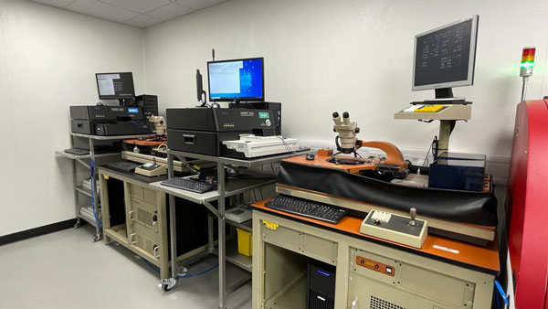
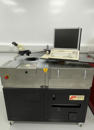
All wafer probing is conducted in-house within a Class 100K or Class 10K (optional) environment.
Our experienced engineers develop individual test programs for each device.
- Test concept development and output format requirement
- Test program development
- Test hardware development
- Test verification
- 100% probing (+ inking if required)
- Data output and documentation
- View our parametric electrical test capability
We also offer other complimentary processes such as wafer sawing and pick and placing to provide a full bare die processing solution.
